- 3876 Industrial Ave, Rolling Meadows, IL 60008
- Info@auctuselectro.com

- 3876 Industrial Ave, Rolling Meadows, IL 60008
- Info@auctuselectro.com
Wire Bonding
- Home
- Wire Bonding
Precision Microelectronic Interconnects with Advanced Wire Bonding Systems
In modern semiconductor packaging, hybrid microelectronics, and high-reliability aerospace sensors, establishing rock-solid electrical connections between silicon integrated circuits (ICs) and substrate lead frames is vital. Traditional soldering methods are far too coarse for delicate microscopic die pads, where thermal stress and flux residue can ruin microscopic circuits. Consequently, implementing high precision Wire Bonding technology has become a fundamental assembly standard for microelectronics manufacturers across the USA. Utilizing ultra-fine gold, aluminum, or copper wire—often thinner than a human hair—this solid-state welding process forms reliable electrical interconnects under precise heat, pressure, and ultrasonic energy. Therefore, leveraging automated micro-interconnect solutions directly protects delicate silicon structures, delivers superior high-frequency signal integrity, and guarantees long-term device performance.
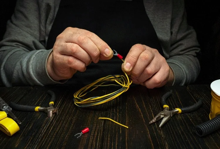
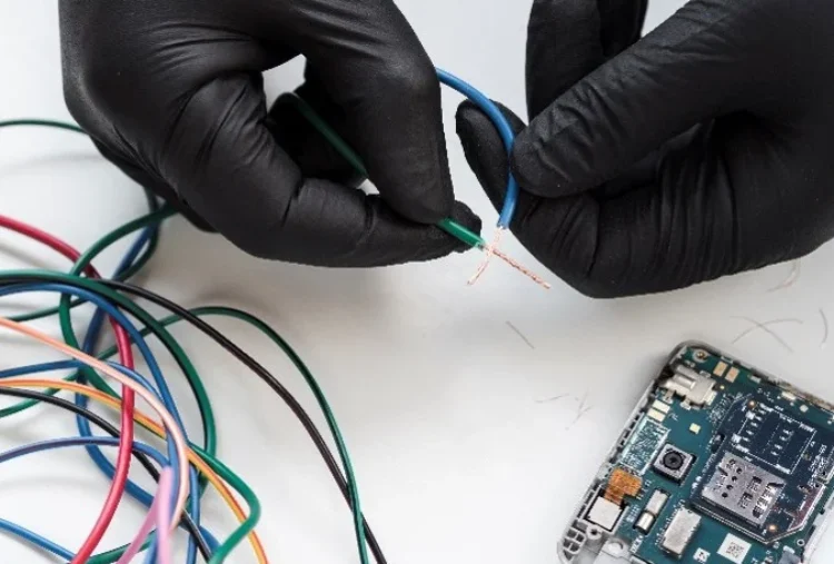
Protecting Delicate Microchips with Solid-State Ultrasonic Welding
Applying high heat or mechanical force directly to fragile silicon dies risks cracking microscopic substrate layers and shorting delicate circuit traces. Furthermore, solder flux contamination on microchip pads causes severe long-term corrosion and bond detachment. However, deploying an automated wire bonding system eliminates these microelectronic assembly risks through low-temperature solid-state welding. By combining precise ultrasonic vibration with controlled capillary pressure, ultra-fine wire forms atomic-level metallic bonds without melting the silicon die. Consequently, your engineering team receives ultra-reliable micro-interconnects ready for seamless integration into Microelectronic Package Assembly Setups with zero thermal die damage.
Technical Variants in Semiconductor Interconnect Processing
Selecting the correct bonding method, metallurgical wire composition, and capillary tooling depends on chip pad pitch, thermal budgets, and package height limits. Understanding these technical approaches helps packaging engineers choose the optimal process for critical microelectronic devices.
Thermosonic Ball Bonding vs. Ultrasonic Wedge Bonding
First, choosing between ball bonding and wedge bonding impacts both processing speed and interconnect geometry. Thermosonic ball bonding forms a microscopic spherical ball at the wire end before welding it to the die pad, offering high-speed, 360-degree loop routing ideal for high-density IC packages. Alternatively, ultrasonic wedge bonding operates at ambient room temperature without heat, making it perfect for heat-sensitive hybrids, aluminum-pad power modules, and low-profile RF packages. Securing this level of micro-welding expertise is straightforward when collaborating with a certified Precision Semiconductor Interconnect Partner.
Metallurgical Wire Selection: Gold, Aluminum, and Copper Alloys
Second, selecting the proper interconnect wire alloy directly influences conductivity, loop stiffness, and manufacturing cost. High-purity gold wire offers outstanding corrosion resistance and soft deformation characteristics. However, copper wire provides higher electrical conductivity and superior thermal dissipation for high-power devices. Furthermore, aluminum-silicon wire remains the industry standard for room-temperature wedge bonding in high-reliability power modules. Matching these alloys with your Custom Micro-Welded Substrate Assemblies ensures optimal electrical performance across demanding operating environments.
Strict Quality Diagnostic Protocols for Micro-Interconnects
Verifying bond adhesion strength and joint integrity is vital for passing rigorous MIL-STD-883 microelectronics reliability audits. Every production lot undergoes structured non-destructive and destructive laboratory testing.
- Non-Destructive Wire Pull Testing: Applies calibrated vertical tension to verify loop strength without damaging acceptable bond joints.
- Ball Shear Testing: Measures the lateral force required to shear the bonded ball off the die pad, confirming complete intermetallic formation.
- Crater Testing and Metallographic Analysis: Audits underlying silicon substrate layers under etched bond pads to verify zero cratering or sub-surface cracking.
- Scanning Electron Microscopy (SEM) Inspection: Inspects bond tail formation, heel deformation, and loop clearance under extreme optical magnification.
Integrating Micro-Bonded Modules into System Assemblies
Building complex industrial sensors or defense electronics requires mounting wire-bonded micro-hybrids into rugged sub-assemblies. To streamline this transition from die level to system level, engineering teams connect micro-bonded packages directly into a complete Micro-Packaging Integration Framework. This unified layout prevents mechanical stress during housing encapsulation and ensures reliable signal transfer to primary control boards.
Complete Circuit Board Fabrication and Enclosure Protection
Modern OEMs demand seamless alignment between micro-bonded silicon dies, main printed circuit boards, and protective environmental enclosures. Contracting a single full-service manufacturing partner simplifies vendor logistics and shortens product development cycles.
Interfacing Microelectronic Packages with Printed Circuit Boards
To maintain low-noise signal transmission, micro-bonded hybrid modules must connect cleanly to surrounding system boards. Linking your micro-packaging workflows with high capacity Printed Circuit Board Assembly Solutions prevents impedance mismatches and stray capacitance issues. Consequently, your processing boards handle delicate sensor signals accurately without experiencing data distortion. This manufacturing integration guards your core processing electronics against signal degradation.
Heavy-Duty Sealed Enclosures and Custom Metal Work
Finally, delicate wire-bonded silicon chips and substrate modules require hermetically sealed physical housing to block moisture, dust, and electromagnetic interference (EMI). Full-service contract partners combine their microelectronic packaging expertise with comprehensive System Engineering and Fabrication. This end-to-end capability allows you to source micro-bonded hybrid modules, main electronic control boards, and NEMA-rated metal enclosures from a single trusted domestic partner like Auctus Electro.
Frequently Asked Questions (FAQs)
1.What is wire bonding in semiconductor packaging?
Wire bonding is a solid-state welding process that uses ultra-fine wire (gold, aluminum, or copper) and a combination of heat, pressure, and ultrasonic energy to create electrical connections between a silicon IC die and its package leads or circuit substrate.
2.What is the difference between thermosonic ball bonding and ultrasonic wedge bonding?
Ball bonding forms a molten sphere at the wire tip before bonding, allowing high-speed, omnidirectional wire looping suitable for dense IC packages. Wedge bonding creates a wedge-shaped weld line without melting the wire end, allowing lower loop profiles and ambient-temperature bonding for heat-sensitive parts.
3.Why is copper wire increasingly used instead of gold wire?
Copper wire offers significantly higher electrical and thermal conductivity compared to gold while being substantially more cost-effective. However, copper requires an inert shielding gas (like nitrogen/argon) during bonding to prevent wire oxidation.
4.What causes wire bond heel cracks or pad cratering?
Heel cracks occur when excessive ultrasonic energy or tight bending weakens the wire transition zone near the wedge weld. Pad cratering happens when excessive bonding force or ultrasonic energy cracks the brittle silicon substrate beneath the metal pad.
5.Where can I source custom microelectronic wire bonding services in the USA?
You can partner with established domestic contract manufacturers like Auctus Electro to submit your hybrid design specifications and receive a comprehensive manufacturing consultation.
Conclusion
In conclusion, mastering high-precision wire bonding is an essential strategy for achieving high-density microelectronic packaging, superior signal integrity, and long-term joint reliability. By prioritizing correct alloy selection, precise ultrasonic energy control, and rigorous MIL-STD-883 pull and shear testing, you eliminate thermal die stress and connection failures. A full-service partner like Auctus Electro delivers microelectronic packaging capabilities, custom assembly expertise, and integrated contract manufacturing support needed to bring your complex hybrid designs into full production reality. Choose an engineered micro-interconnect solution that drives your product reliability forward with absolute accuracy and confidence.
Go To Top